PIERD(Patented)

About PIERD: Innovative Symbol Mark Technique

Choose PIERD instead of no-reference-designators!

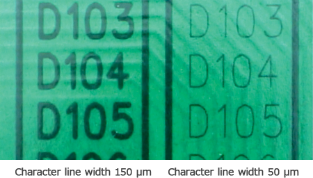
In recent years, the minimization and densification of electronic parts are rapidly advancing. Because of that, the thickness of the references (such as letters and symbols) on PWB has an impact on mounting electronic components.


Therefore, we sometimes see PWBs without references in some situations. There is an advantage due to the absence of references, on the other hand, the role introduced by the references is also important for maintenance etc..


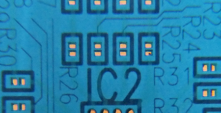
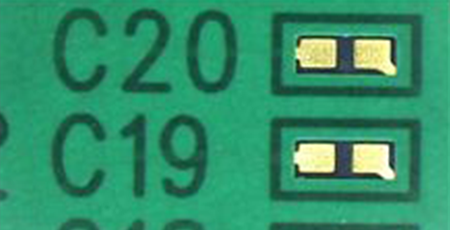
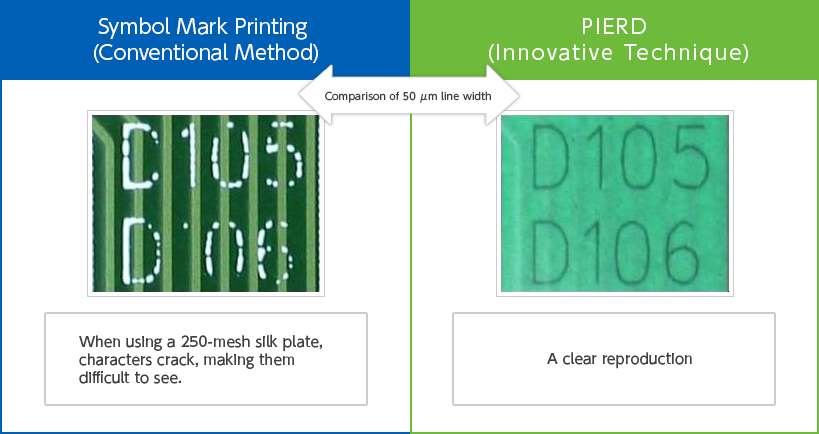
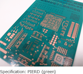
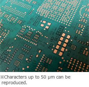
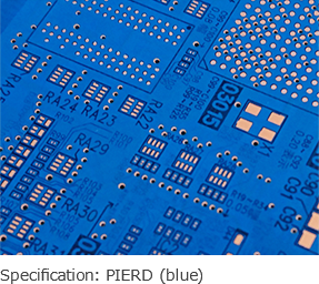
Our patented technology is called PIERD which has the advantages of both PWB with references and one without references. PIERD makes it possible to express characters and symbols on the solder mask in the way that silk screen printing can not do. Also, there is feature that there are few restrictions for the placement of the character.


In addition, the number of direct imaging machine used for the solder mask has been gradually increasing at manufacturing sites. If you use the machine, you can place the serial number etc. on the PWB. This feature is expected to use for improving traceability.

Patented (Patent No. 5374799)
PIERD現像型組み込みリファレンス
We received the "JPCA Award" at the 44th Japan Electronics Packaging and Circuits Association Show. (2014)

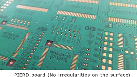
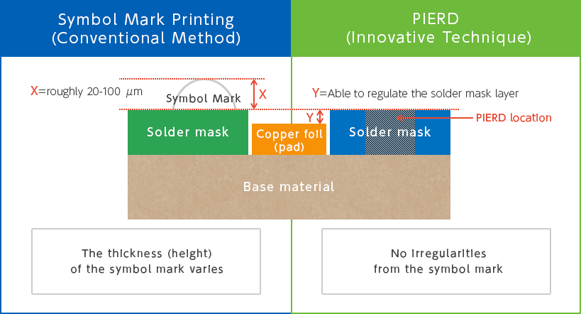
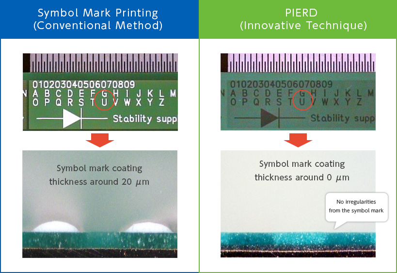
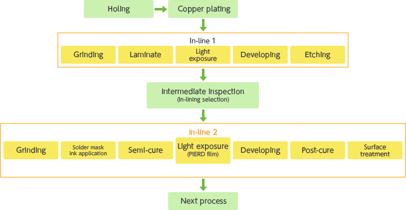
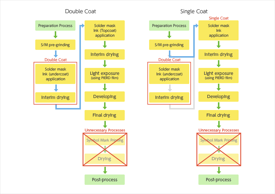
At this time, the patent has been acquired for innovative symbol mark technique PIERD.This new technique is not a conventional printing method, but uses light exposure to inscribe a symbol mark within the solder mask layer.


Eliminating the need for Symbol Mark Printing, it inscribes smooth symbol marks without irregularities, with excellent resolution and high positioning precision.

About PIERD

PIERD Product

We incorporate a recognizable image within the coated thickness of the solder mask.

  • PIERD board (No irregularities on the surface) 
  • PIERDの詳細画像
  • PIERDの詳細画像
  • Character line width 150 μm Character line width 50 μm

Comparison of Conventional Symbol Mark Printing and PIERD

PIERD シンボルマークにおける新工法 PIERD シンボルマークにおける新工法 PIERD シンボルマークにおける新工法

Merits of PIERD

Merit#1
Symbol (Characters / Symbols)
  • Via photo method inscribed in the solder mask (no wearing or scratches
  • No irregularities (effective for mounting microchips
  • Monochrome image formation possible (Gradient expression possible
  • No smudging, wearing or pad fogging (A much lower defect rate than Symbol Mark Printing
  • Improved implementation reliability (Achieves "0" number of character defects
Excellent Resolution and High Positioning Precision
  • Able to inscribe clear images at line width 30 μm
  • The reference can be made at the actual location (reducing printing space restrictions
  • PIERD can make two dimensional codes such as barcodes or QR codes etc. (A useful tool for information transmission and process control: can identify product lot
QRコード等の2次元コード
メリット02
Reduction (or Elimination) of the Number of Processes in Symbol Mark Printing
  • Workers highly skilled and experienced in printing no longer needed
  • Reduction of processing panels
  • Version control and storage no longer necessary
  • Reduction of consumable materials and organic solvents used in the manufacturing process
  • Improved status control by reducing manufacturing steps
  • Reduction of electricity costs
メリット03
Fully Functional with Existing Equipment
  • Completely unnecessary to introduce new equipment to support PIERD
  • Light exposure processing done once (provided that PIERD film is used)
  • In PIERD film data processing, solder mask and symbols are processed on the same side of the film sheet.
メリット04
Green Procurement
  • Plate frame (Aluminum) no longer necessary thereby reducing CO2
  • Reduction of CO2 emissions by lowering electricity costs for drying furnaces
  • CO2 reduction by lessening Symbol Mark Printing processes, equipment and secondary materials
  • CO2 reduction by reducing organic solvents
  • CO2 reduction by reducing personnel
UL Environment
  • No change in procedure (However, additional registration of PIERD ink is necessary)
メリット05
In-lining (Substantial Productivity Improvement
  • No need for the prep and post processes that limited in-lining in Symbol Mark Printing.
  • Direct connection between the solder mask process and surface treatment (Heat resistant pre-flux & horizontal leveler).
  • Circuit formation ⇒ Solder mask process ⇒In-lining the surface treatment process.
インライン化(大幅な生産性改善)

開発の歩み

PIERD Development History

PIERD シンボルマークにおける新工法PIERD シンボルマークにおける新工法

Regarding Process Methods - Comparison between Double Coat Method and Single Coat Method -

PIERD シンボルマークにおける新工法

Product Line

  • Specification: PIERD (green)
  • ※ Enlarged photo on the left Characters up to 50 μm can be reproduced.
  • Specification: PIERD (blue)
For
TSK Inc.
TEL 0573-25-4414
Manager: Sales department Mr.Nishio
E-mail: k-nishio◆tsk-pcb.co.jp
* When sending emails, please replace the ◆ mark with an @ mark.
PAGETOP