プロセス

At our company, all work processes are in-house and integrated, allowing us to accept anything from prototypes to mass production.

All equipment supports integrated in-house production, for example, automatic plating lines, multilayer press machines, etc. are prerequisite to shorting set up times.From making a single prototype we deliver product development in a short time, supporting all the steps to low-cost mass production.

AOIによる
厳しい品質管理体制
Strict Quality Control Through AOI
AOIによる
厳しい品質管理体制
High Level Technology, Capable of High Density Wiring
AOIによる
厳しい品質管理体制
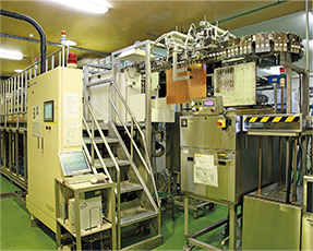
Accepting Orders from Prototypes to Mass Production
AOIによる
厳しい品質管理体制
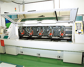
High Precision Etching with Ferric Chloride-based Solution
AOIによる
厳しい品質管理体制
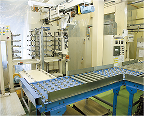
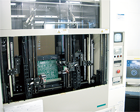
Vertical Carrier Jet Type Fully Automatic Plating Ensures High Level Uniformity in Mass Production
AOIによる
厳しい品質管理体制
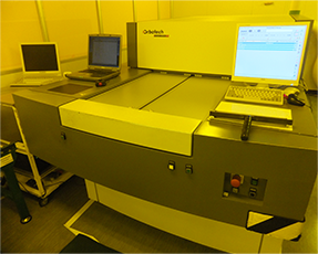
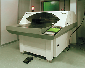
High Speed / High Accuracy PWB Automatic Inspection

Steps to Delivery

  • 1
    Data Editing
    Editing of Garber data sent from clients, creating working films as well as NC data / Router Data etc.
  • 2
    Inner Layer Process
    Carrying out Inner layer pattern formation / etching inspection / blackening etc.
  • 3
    Vacuumed Multilayer Pressing
    Combining several inner plates to form a vacuum while pressing and applying heat from the oil heater.
  • 4
    Holing
    NC machines make holes (holes for inserting components and holes for electrical continuity).
  • 5
    Smear Removal
    Smear removal of epoxide resin generated when holing.
  • 6
    Copper Plating
    Copper plating is applied to the whole PWB surface (outer surface and inner hole walls) to electrically connect the front and back.
  • 7
    Hole Plugging
    When etching, in order to protect the copper plating in the holes from the etching solution, resin is embedded within the holes and hardened with UV.
  • 8
    Belt Grinding
    Smoothing of the surface to maximize adhesion of the etching resist.
  • 9
    Pattern Formation
    As an etching resist, dry film is laminated, then light exposure and developing are done.
  • 10
    Etching
    Other than the desired conductor pattern protected by the etching resist, unnecessary copper foil parts will be removed by the etching solution.
  • 11
    Intermediate Inspection (by AOI)
    Scanning the pattern optically, we inspect for the presence or absence of defects (breaks, short circuits, cracks, thick and thin circuits etc.).
  • 12
    Solder Mask
    When soldering electronic devices etc., permanent masking of the surface pattern for the purpose of protecting it from the external environment and to prevent soldering of unnecessary parts.
  • 13
    Symbol Mark Printing
    Printing of the position of parts to be mounted, the product name etc.
  • 14
    Surface Treatment
    Protecting copper foil areas on the surface of the PWB where resist is not applied.
    The methods are; Pb-free, Solder Leveling, OSP, and Gold Plating.
  • 15
    Blanking and Routing
    Blanking and routing with an NC router or a mold press.
  • 16
    Test
    •Dedicated jig: Conducts continuity test for mass production products.
    •Flying Probe Tester: Conducts continuity test by a moving probe for prototypes and small lot production products.
  • 17
    Inspection / Delivery
    The appearance etc. is checked, and items that pass inspection are packed into a box and delivered to the destination specified by the customer.

Examples of Large Machines

  • DI(ダイレクトイメージング)
    Laser Direct Imaging(LDI) system
  • 真空積層プレス
    Vacuumed Multilayer Press System
  • NC穴明け機
    NC Drilling Machine
  • 硫酸銅めっき
    Sulfuric Acid Copper Plating System
  • インクジェット・シンボル印刷機
    Inkjet / Symbol Mark Printing System
  • 導通検査(フライングチェッカー)
    Flying Probe Tester
PAGETOP